The smartest feature in a pair of display-equipped AI glasses is useless if the optical part cannot be made at a price people will pay. That is the less glamorous side of wearable computing: not the assistant answering a question, but the factory reproducing the tiny structures that put an image in front of your eyes. Morphotonics is selling a way to repeat that work across larger manufacturing surfaces. Its latest financing puts a specific industrial bet behind the enthusiasm for glasses.
On September 22, The Next Web reported that the Dutch equipment company had raised more than 40 million euros in an expanded Series B. The report names returning investors 3M Ventures, Innovation Industries and BOM, with Invest-NL joining as a major new backer. It describes spending on production capacity, product development, staffing and support. The funding total is reported, not independently reconstructed from financing documents by this publication. It should not be read as proof that all of that money arrived in one transaction this morning.
The company's original announcement provides useful context. On September 11, 2024, Morphotonics disclosed a first Series B close above $10 million and anticipated another closing. The current report describes an extension of that round. Adding the dollar figure to the euro figure would manufacture a larger fundraising total without establishing whether the amounts overlap. More useful than that arithmetic is the continuity of the plan: the earlier capital was already intended to expand operations, supply chains and display-optics manufacturing.
The underlying process is nanoimprint lithography. In Morphotonics' explanation, a precision stamp physically transfers a surface pattern into a soft material. Ultraviolet light hardens the resin, and the stamp separates, leaving the pattern behind. Think replication rather than drawing every feature from scratch. The difficult work does not disappear; it moves into creating the master, controlling the materials and making each copy faithful enough for its intended use. The company's process is an approach to manufacturing optical structures, not evidence that every kind of chipmaking can be replaced by a roller.
Its roll-to-plate method progressively presses a flexible stamp across a panel. That differs from roll-to-roll processing of a continuous flexible film. The company describes compatibility with rigid and flexible substrates, including glass and polymers, and two possible roles for the transferred pattern: it can remain as an optical layer or serve as a mask for subsequent etching. Those alternatives matter because a manufacturer's next processing step determines what the imprint must survive and what characteristics the resin needs.
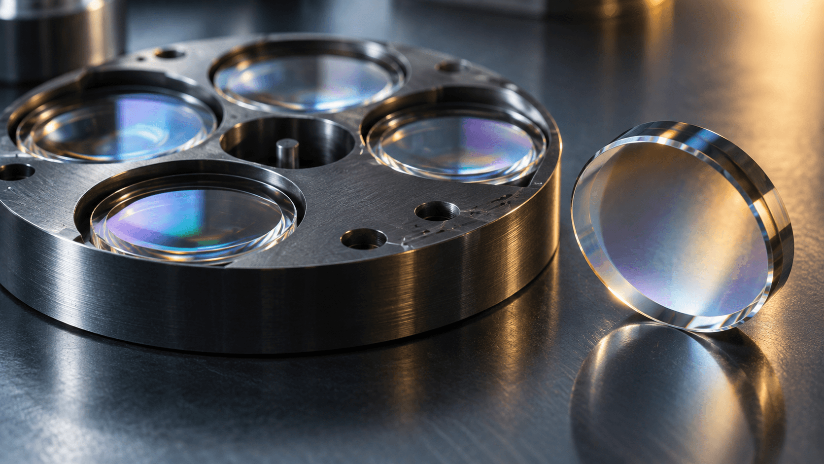
For display glasses, the relevant component is a waveguide, the transparent optic that helps deliver the digital image to the wearer. The attraction of nanoimprinting is the ability to reproduce the small surface structures used in that optical design. But reproducing a shape and delivering a good viewing experience are different acceptance tests. A purchaser should specify the optical result it needs, not merely the presence of a convincing microscopic pattern. That is a procurement recommendation, not a claim that Morphotonics' customers have accepted poor parts.
The Cypris X700 brochure makes the scale proposition concrete. Morphotonics advertises capacity of up to six million eyepieces annually and a possible four-minute manufacturing cadence that depends on product texture. It lists carriers handling four 300-millimeter round wafers or nine 200-millimeter wafers, within a handling area up to 700 by 700 millimeters. These are supplier specifications. They do not establish how many accepted parts a particular customer has produced, how often its line stops or how much of that stated capacity becomes saleable output.
The word eyepieces also deserves to stay intact. An equipment capacity expressed in optical components is not automatically the number of complete glasses a brand can ship. Other parts and assembly operations still belong to the finished product. For someone evaluating the machine, the practical request is an application-specific capacity model: which design, which carrier arrangement, which processing recipe and which acceptance standard produced the estimate? A large annual number without those assumptions is a sales headline, not a production commitment.
An older Morphotonics white paper explains the physical logic behind the larger format. Its illustrated example starts with a single waveguide master, expands that to a submaster carrying 30 waveguides, then shows larger production formats accommodating 120 to 270. This is product tiling: repeat the pattern across more useful area in one manufacturing operation. The example is a company illustration, not a universal promise for every waveguide geometry. It shows why the size of the manufacturing surface can become economically important even when the features themselves are extremely small.
Tiling also creates a question that a buyer should test directly. If more parts share a process step, a process problem could affect more parts together. That is a general consequence to investigate, not a reported defect in these machines. Qualification should examine variation across the carrier and across repeated runs, rather than accepting the best sample from the easiest location. The benefit of larger-area replication is strongest when the quality distribution stays useful across that area, not just when the equipment can hold more glass.
The platform extends beyond the imprint mechanism. Morphotonics describes Cypris as combining nanoimprinting with inkjet printing, robotic handling and multi-wafer carriers. Its broader product range also includes separate primer, coating and imprint modules. Those distinctions give a customer different integration questions. Does it need a complete manufacturing sequence, or one operation inserted into an existing line? What will happen before the imprint and immediately after it? Buying the wrong boundary around the process could leave the customer paying to solve integration work twice.
Materials are part of that boundary. The company supplies its own ultraviolet-curable resins and flexible stamps, alongside software intended to monitor and adjust production. Its product page reports demonstrated stamp lifetimes above 1,000 imprints. That remains a supplier claim, not a lifetime guarantee for every pattern and material combination. A buyer should ask how replacement criteria are measured and priced. Waiting for a stamp to fail visibly is a different maintenance policy from replacing it before output drifts outside an agreed optical specification.
There is a real commercial tradeoff here. Getting equipment, materials and process support from one supplier may make troubleshooting more coherent: fewer organizations can argue that the problem belongs somewhere else. It can also increase dependence on that supplier's formulations, replacement parts and service. Neither outcome is inevitable. The useful contract questions concern approved alternatives, access to process records, support response times and what happens if a consumable changes. These are proposed diligence questions, not claims about restrictions in Morphotonics' undisclosed customer agreements.
The company's AR application brochure reinforces why the recipe matters. It describes compatibility with several grating shapes, high-refractive-index and etch-resist resins, coating alternatives and downstream operations including etching and atomic layer deposition. That is a menu of process possibilities, not a claim that every combination performs identically. A developer choosing materials should qualify the complete sequence it intends to use. A successful imprint before downstream processing is not, by itself, proof that the final optical component meets the product requirements.
Morphotonics' lab-to-fab network is designed to let customers explore those questions before buying equipment. The company identifies different partner roles: Temicon supports European pilot work and production scaling, CSEM connects research with technology transfer, and Moveon supports the progression toward commercial manufacturing in Asia-Pacific. These are the network's stated capabilities, not a guarantee of available capacity or a delivery date. The access model is nevertheless relevant to a startup that needs manufacturing evidence before it can justify owning a line.
A sensible trial would end with more than attractive samples. It should leave the customer with a documented design, material specification, processing sequence, measured output and an explanation of which assumptions change at higher volume. That would make the pilot useful to both the engineering team and the person authorizing the equipment purchase. Otherwise the company risks buying a demonstration twice: once as a service, then again as machinery that still needs its production process developed.
The Next Web also reports ambitions beyond glasses, including photonic components for future data centers and co-packaged optics. That is an adjacent opportunity, not a demonstrated data-center manufacturing business in the evidence reviewed here. The important test is whether a specific component actually benefits from this replication process and passes the requirements of its intended system. An optical technology does not become interchangeable with every other optical technology simply because both involve light.
For the business, that distinction argues for disciplined expansion. A manufacturer can explore another market without asking its existing customers to subsidize an unrelated development program indefinitely. The questions are concrete: which capabilities transfer, which require new tooling, and who funds qualification? The public material reviewed does not provide application-level margins or the costs of entering each new market. Any claim that the data-center opportunity has already transformed Morphotonics' economics would go beyond the available record.
The strongest case for the company is not that AI glasses are certain to win. It is that a difficult production step may support an equipment-and-process business across multiple customers. The counterargument is equally practical: even a capable manufacturing platform needs designs worth manufacturing and customers prepared to commit. Better replication cannot rescue a wearable that people dislike wearing, or a product whose economics fail elsewhere. Those are commercial conditions, not a forecast of failure.
For builders, the financing is a reason to investigate the manufacturing route, not to erase manufacturing risk from a roadmap. Ask for evidence on your optical design, your materials and your required output. Keep supplier capacity claims separate from accepted production results. The next compelling development will be a customer showing that this process delivers the right optics at a sustainable cost. That would make the wearable opportunity more tangible than another assistant demo ever could.
LaunchPad positionQualify optical output on the intended design and materials before treating advertised equipment capacity as a product shipment plan.
This report draws on the linked primary sources and reputable reporting. Company statements are treated as claims until independently demonstrated.